Optoelectronics detect or emit light and are used in a variety of devices in many different industries. These devices have historically relied on thin transistors, which are small semiconductors that control the movement of electrons and photons made out of graphene and other two-dimensional materials. However, graphene and these other materials often have problems with band gap opening and other shortcomings that have researchers searching for an alternative.
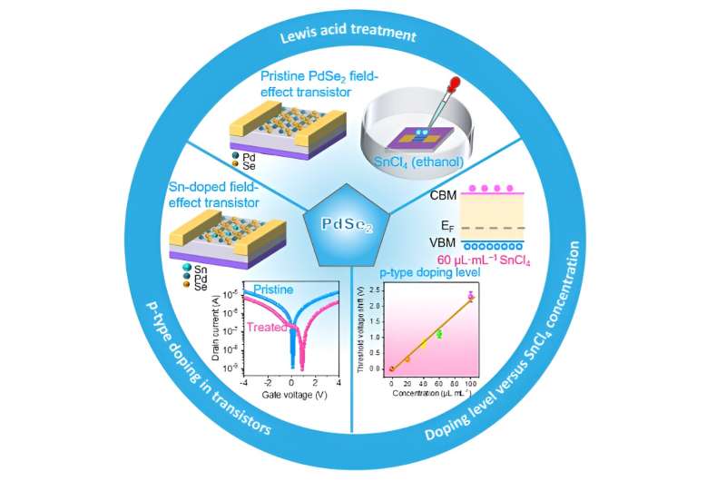
When treated with a method called the Lewis acid treatment, palladium diselenide is a possible solution to satisfy the needs of optoelectronic devices.
Research analyzing this method was published in a paper in Nano Research.
Prof. Dr. Mark H. Rümmeli, ERA Chairs professor at the Technical University of Ostrava (VSB-TUO), said, “Palladium diselenide exhibits unique physical properties, including a tunable band gap and impressive device performance. Notably, it demonstrates long-term stability in ambient air without the need for additional packaging.”
Inspired by semiconductor physics, the researchers considered how doping might alter palladium diselenide to improve its performance. Doping is the intentional introduction of impurities to a material, resulting in three types of materials: pristine, p-type doped, and n-type doped. When a p-type doped material and an n-type doped material touch, they create a p-n junction. This junction is essential for optoelectronic devices because it is where light-to-electron and electron-to-light conversion occurs.
To create p-type doped and n-type doped palladium diselenide in a controlled fashion, researchers used the Lewis acid treatment. “The controlled level of doping can make palladium diselenide have a different energy bandgap, which enriches a toolkit or library of materials for the selection and design of the p-n junction,” said Dr. Hong Liu, a professor at the State Key Laboratory of Crystal Materials at Shandong University in Jinan China.
“The Lewis acid treatment can introduce the substitution of the palladium atoms (by tin from tin chloride, one type of Lewis acid) in the palladium diselenide. We found a data fitting equation between the doping level versus the concentration of Lewis acid, which may inspire people to manipulate more p-type doped two-dimensional materials.”
In order to test this method, researchers prepared a pristine film of palladium diselenide. The film was then modified using the Lewis acid treatment. After the initial Lewis acid treatment, the lattice structure of the palladium diselenide film was unchanged, but emerging peaks of tin, palladium, and selenium were confirmed using imaging.
These peaks proved that tin could be used as a p-type dopant. Additional tests of different concentrations of tin chloride showed how the threshold voltage of the palladium diselenide could be controlled depending on the concentration of the tin chloride. These guidelines can be applied for future doping of palladium diselenide using Lewis acids. It could also provide a blueprint for how to do similar testing on other semiconductor materials.
Looking ahead, researchers will plan how to scale the processing of these two-dimensional materials. “We will demonstrate the exciting applications of p-type doped palladium diselenide in several electronic components, such as field-effect transistors, photodetectors, and light emitters. We plan to try to optimize the semiconductor doping method, which can be readily adopted by the industrial standards and could be employed in the semiconductor industry for mass production in the near future.”
“Our ultimate goal is to apply this technique in wearable and flexible electronics by integrating the palladium diselenide-based transistors and photodetectors with polymer-based strain sensors in flexible substrates, which result in a smart biomedical system for human health care monitoring applications,” said Dr. Jinbo Pang, a professor of chemistry and materials science at the University of Jinan in Jinan, China.
More information:
Jiali Yang et al, Modulating p-type doping of two dimensional material palladium diselenide, Nano Research (2023). DOI: 10.1007/s12274-023-6196-7
Journal information:Nano Research
Provided by
Tsinghua University Press

READ MORE
5 Ways to Dress to Impress at Your Next Job Interview
You may have gotten used to spending time at home for work or maybe you [...]
This Pacific Coral Can Withstand Warming Waters With the Help of Algae
Antler coral can host different types of algae, sometimes resulting in differences in color. Thomas [...]
Can Scientists Forecast Algal Blooms and Pest Outbreaks Like We Do the Weather?
Images created by NASA with satellite data helped the U.S. Department of Agriculture analyze outbreak [...]
DNA computer using glass beads increases parallel processing power
Schematic of DMOLs detecting the presence of a chemical input. Credit: Nature Nanotechnology (2022). DOI: [...]
All the Gold in the Universe Could Come From the Collisions of Neutron Stars
Two neutron stars violently collide—potentially the sourse of all heavy elements in the universe, including [...]
A gold electrode fabrication technology that can be combined with thermotherapy technology based on photothermy
Graphical abstract. Credit: ACS Applied Materials & Interfaces (2023). DOI: 10.1021/acsami.3c01160 DGIST Professor Hongki Kang [...]
Elusive prickly sharks spotted gathering at underwater mountain off Panama — but why remains a mystery
Researchers have spotted an atypical gathering of rare prickly sharks around a seamount off Panama. [...]
Why Do You Need A Mobile Phone Insurance Plan?
Mobile phones and smartphones are now an integral part of our everyday lives. More than [...]